Memory Hierarchy, Revisited
Learning Outcomes
- Define key components of the memory hierarchy: processor, caches, memory, disk.
🎥 Lecture Video: Memory Hierarchy
Ideally one would desire an indefinitely large memory capacity such that any particular … word would be immediately available. … We are … forced to recognize the possibility of constructing a hierarchy of memories, each of which has greater capacity than the preceding but which is less quickly accessible.
— Preliminary Discussion of the Logical Design of an Electronic Computing Instrument (1946)
Memory Wall
While hardware performance has continued to improve, there is a persistent and increasing gap between the improvements in processor hardware and memory/device interconnects (the Processor-DRAM gap, or simply memory gap).1 The “memory wall”2 places a significant limit on performance for many modern workloads, especially in AI.3
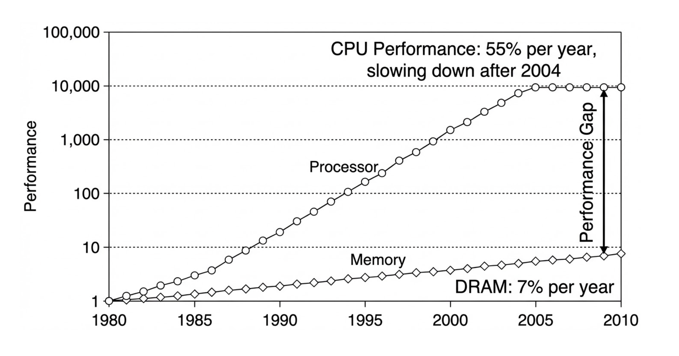
Performance gap between DRAM and CPU.
By designing a memory hierarchy, we can leverage smaller amounts of high-speed hardware without ballooning the cost of our architecture nor sacrificing data and storage capacity.
The Memory Hierarchy, Revisited
Earlier, we assumed there were only two layers of our memory hierarchy: registers (on the CPU) and memory (DRAM is close, but on a separate chip). We now continue our earlier discussion of memory hierarchy.
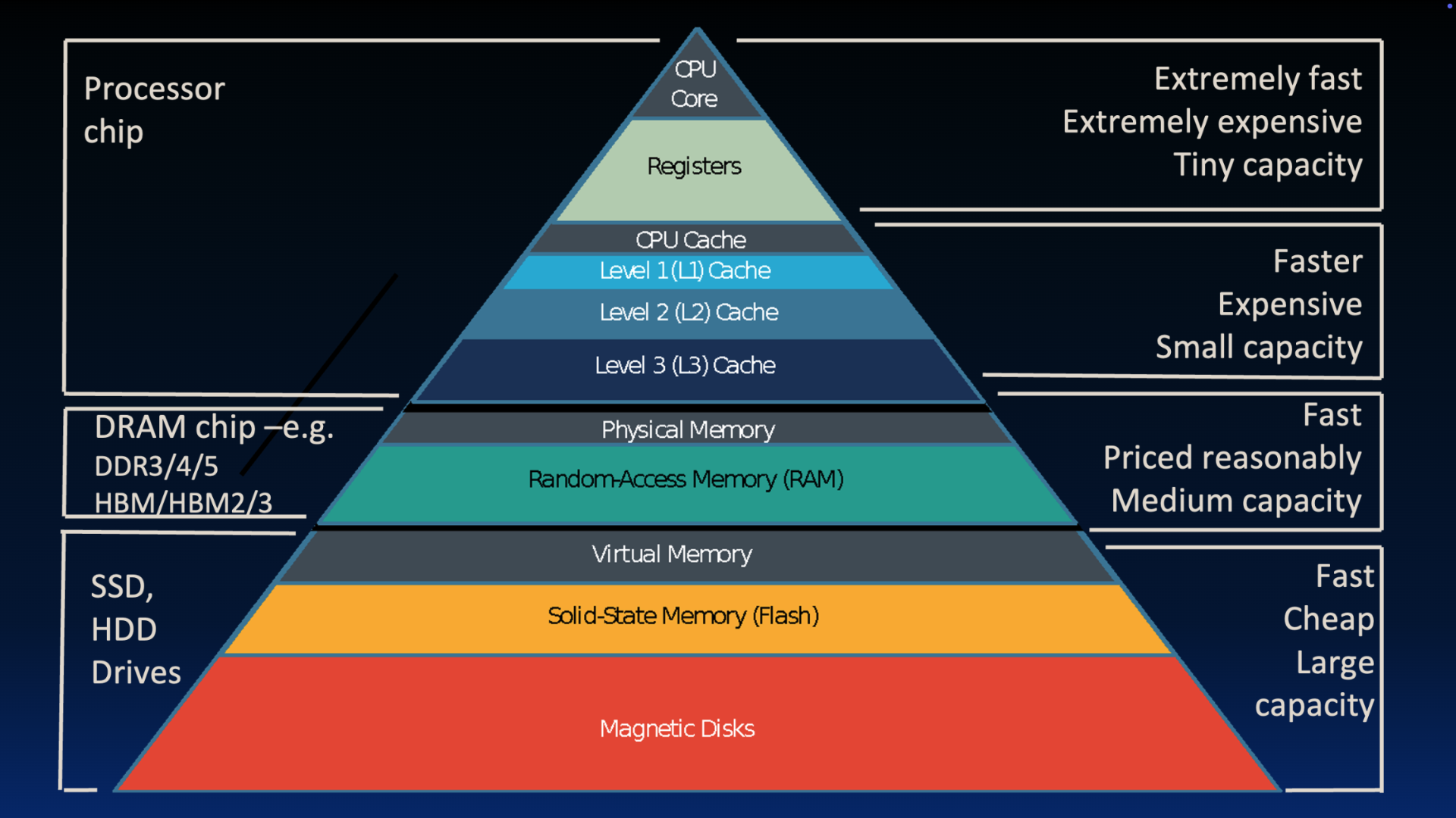
Great Idea 3: The Principle of Locality / Memory Hierarchy
The mismatch between processor and memory speeds (the “careful tango” described earlier leads us to add a new level: The memory cache, or cache for short. Caches are usually on the same chip as the CPU and fit into the memory hierarchy as follows:
- Size: Smaller than memory, but certainly larger than the 32 registers on our RISC-V processor.
- Speed: Use hardware that is much faster than DRAM (used for main memory), but slower than registers.
- Cost: Use hardware that is more expensive than DRAM.
There are additional levels lower than main memory: disk is a huge one (literally).
Data moves differently between different levels of the memory hierarchy:
- Registers and memory: Managed by the compiler. Loads and stores move data in and out.
- Cache and memory: Managed by cache controller hardware. We will describe the high-level operation, but leave the implementation to a later course.
- Memory and disk: Managed by the operating system and special hardware via virtual memory, a concept we discuss later. Additionally managed by the programer/user via files and file streams.
To summarize, we aim for the illusion of a “very large and fast memory”:
- We make memory fast by using a hierarchy, where higher levels use faster, smaller, and more expensive hardware and are located physically closer to the processor.
- We make memory large by leveraging the principle of locality by “caching” the “right” data in higher levels, and delegating lower levels to store more data. The lowest level contains all available data (though nowadays we don’t go to magnetic disk and stop at SSD).
If useful, we revisit Jim Gray’s analogy of data access time on registers, on the cache, in main memory, and on disk.
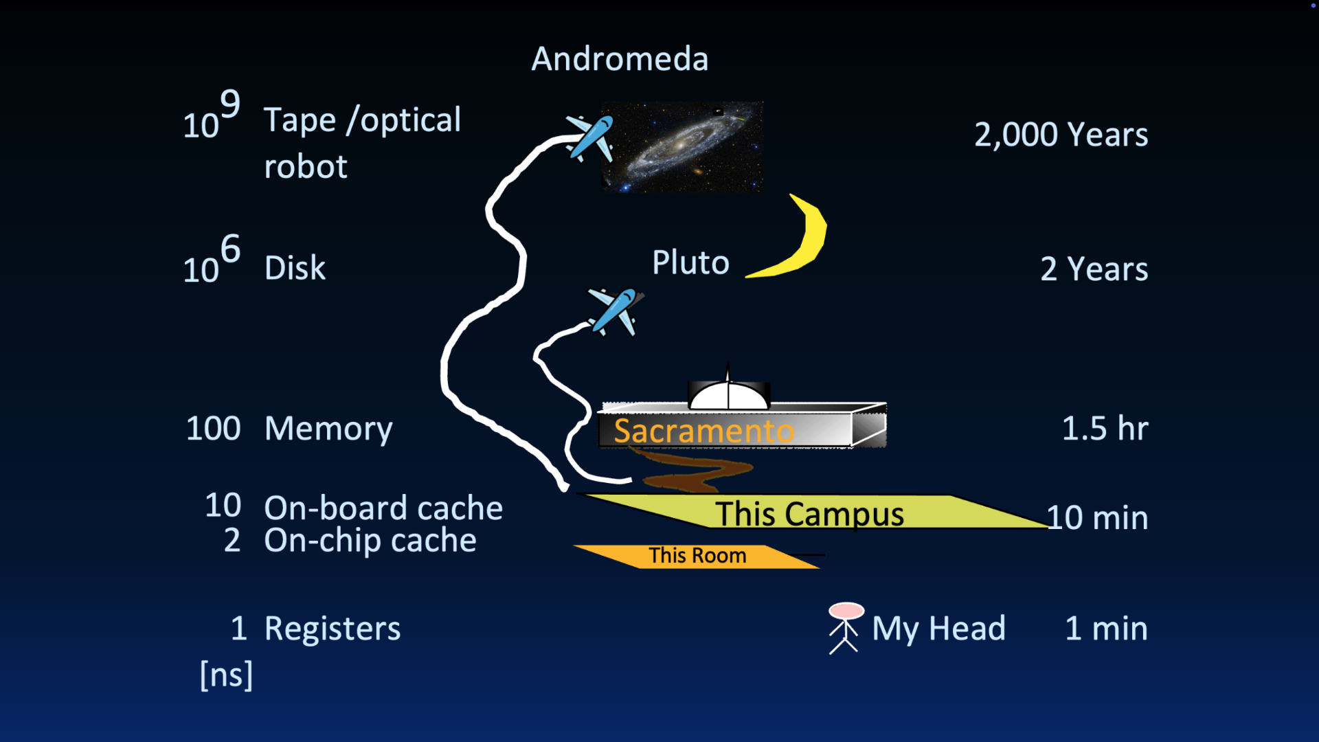
Great Idea 3: The Principle of Locality / Memory Hierarchy
Multi-Level Caches
You may have noticed that the memory hierarchy diagram contains multiple caches labeled Level 1, Level 2, and Level 3. A computer can have multiple caches, where each cache is a copy of data from lower in the memory hierarchy.
Consider Apple’s A14 bionic chip, which we introduced earlier:
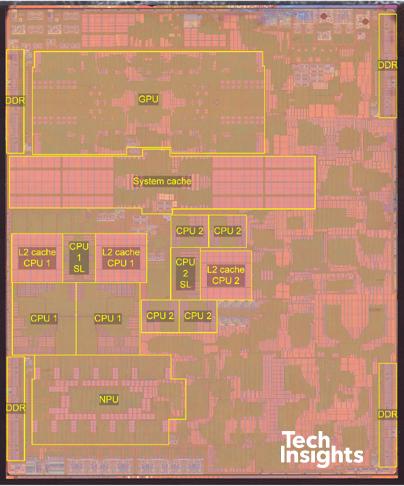
Apple A14 Bionic Chip (sources: Wikipedia, TechInsights)
The L2 cache is located on the integrated circuit, often adjacent to the CPU. The System Level Cache labeled in the diagram is likely a Level 3 cache, shared across multiple CPU cores.4
- L1 cache (L1$5): Usually directly embedded on the CPU, hence why it is not labeled in the above diagram.
- Size: Tens or hundreds of KiB.
- Hit Time (see cache terminology): Complete in one clock cycle or less.
- Miss rate (see cache terminology): 1-5%
- L2 cache (L2$): Located on the integrated circuit, often adjacent to the CPU.
- Size: Tens or hundreds of MiB.
- Hit Time: Few clock cycles
- Miss rate: 10-20%
Demo
To find out the sizes of different components of the memory hierarchy on a Linux-based machine, we can use df and sysctl. The following commands were run on a Mac OS X machine.
To determine disk size, use df. The default display is in blocks (e.g., lines); use the -h option for IEC prefixes (base-two), and the -H option for base-10 prefixes.
$ df -h
Filesystem        Size    Used   Avail Capacity iused ifree %iused  Mounted on
/dev/disk3s1s1   460Gi    17Gi    38Gi    31%    427k  395M    0%   /
devfs            215Ki   215Ki     0Bi   100%     744     0  100%   /dev
...
$ df -H
Filesystem        Size    Used   Avail Capacity iused ifree %iused  Mounted on
/dev/disk3s1s1    494G     18G     40G    31%    427k  395M    0%   /
devfs             220k    220k      0B   100%     744     0  100%   /dev
...
To determine cache size and memory size, use sysctl. Because this command lists all attributes of the system kernel, we pipe the output through grep to get what we want. The default unit is bytes for memory and caches.
$ sysctl -a | grep hw.memsize
hw.memsize: 25769803776
hw.memsize_usable: 25143640064
$ sysctl -a | grep "hw.l.*size"
hw.l1icachesize: 131072
hw.l1dcachesize: 65536
hw.l2cachesize: 4194304Solution
D.
Storage
🎥 Lecture Video: Storage
🎥 Lecture Video: Actual CPUs
🎥 Lecture Video
Written version coming soon, but not too soon. For now, know the following technologies:
- Caches use SRAM (static random access memory).
- Primary storage is memory. Technology used is DRAM (dynamic random access memory), often called RAM.
- Second storage is disk. Technology used is SSD (solid-state drive), though in the past magnetic disks (hard drives) were also common.
Footnotes
-
Maurice Willes. “The memory gap and the future of high performance memories.” ACM SIGARCH 2001. DOI: 10.1145/373574.373576 ↩
-
Wm A. Wulf, Sally A. McKee. “Hitting the Memory Wall: Implications of the Obvious.” ACM SIGARCH 1994. DOI: 10.1145/216585.216588 ↩
-
Amir Gholami et al. “AI and Memory Wall.” IEEE Micro Journal 2024. Extended version on arXiV. DOI: 10.1109/MM.2024.3373763, arXiV:20403.14123/ ↩
-
We don’t discuss L3 caches much in this course. See Wikipedia. ↩
-
The notation
$for cache is a Berkeley innovation. Not me :-) ↩