Control Logic Design
Learning Outcomes
- Given an instruction, identify control signals.
- Explain how a ROM can be used in control logic to translate instruction bits (“address input”) into control signals (“word output”).
- Implement control logic with ROM and combinational logic blocks.
🎥 Lecture Video
In this section we discuss how to implement the controller, i.e., the control logic block. Here is #fig-five-step-single-cycle-control from our chapter introduction to jog your memory.
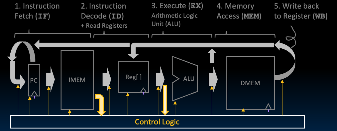
As the datapath computes values, the control logic selects the necessary values needed to execute the instruction.
Review Control Signals
Before continuing, review the following video, which practices identifying and setting the control signals that set the datapath operation for two different instructions: sw and beq.
🎥 Lecture Video
Then, confirm the control signals for the subset of instructions shown in #tab-control-truth-table.
Remember that branches conditionally update PC based on the output of the branch comparator block. The block’s output signals BrEq and BrLT are fed into the control logic, which then sets PCSel selector that wires into the PCSel mux. See the partial truth table below (@tab-branch-truth-table).
Control Logic / Controller
The control logic subcircuit (i.e., the controller) takes the instruction bits (and BrEq, BrLT) and outputs all the control signals needed to execute that instruction. The control signals are listed in #tab-controller-signals.
In general, there are two approaches to implementing control logic:
-
Read-Only Memory (ROM): A ROM reads out words at a given input address. Because the ROM is read-only, it is populated with the needed ones and zeros at design time.
The regular structure of a ROM means it can easily designed and reprogrammed to fix errors (e.g., during prototyping) or when adding instructions (like extensions for compressed instructions). ROMs are also popular when designing control logic manually, like in this course.
-
Combinational Logic using AND, OR, and NOT gates. In real chip design, control is typically designed with logic gates because it is more compact and much faster than ROM alternatives. Today, chip designers use logic synthesis tools to convert truth tables to networks of gates. See this approach below.
ROM Approach
In this course, we implement the controller design in #fig-control-design, which has two subcircuits:
-
Read-Only Memory (ROM): The ROM takes in a 9-bit address constructed from the instruction bits, then outputs a 14-bit “word” that can be decoded into the needed control signals.
-
The Take branch? combinational logic block takes in the Branch Comparator outputs and outputs the
PCSelcontrol signal.
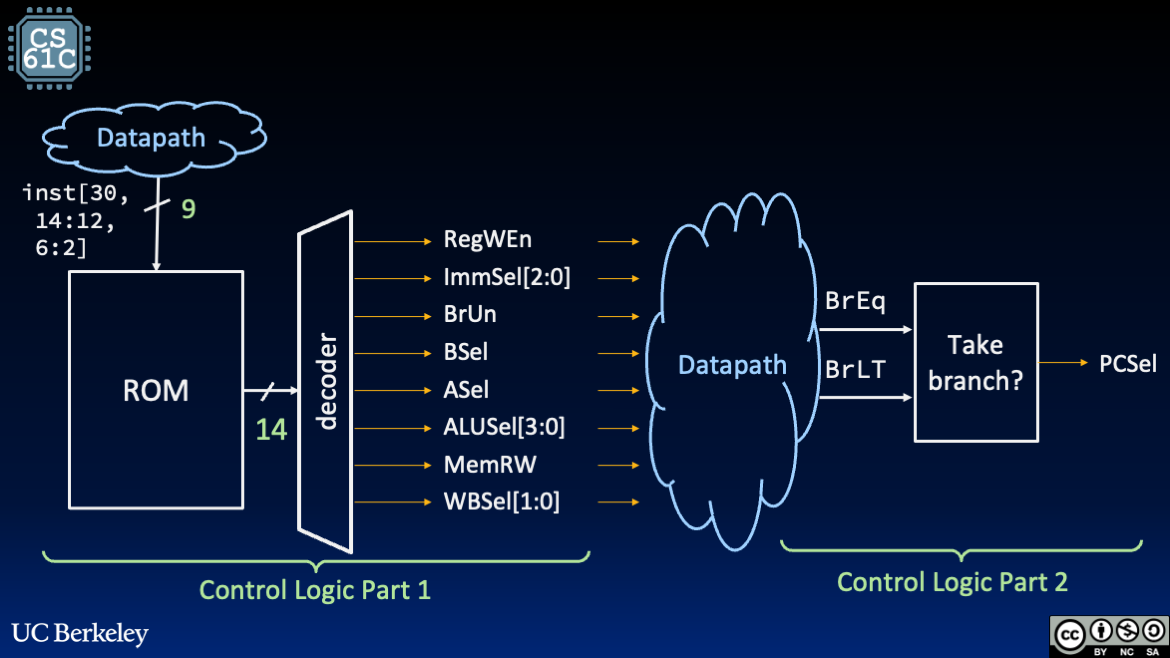
Suggested control design has two parts.
Show Answer
By reducing the address input, we can reduce the size of our ROM.
In RV32I, the instruction type is defined by the fields opcode, funct3, and funct7, where the latter two are present based on instruction format type. This would imply a 17-bit-wide address to our ROM.
However, upon closer inspection, we realize that several of these bit fields are redundant, resulting in a “9-bit ISA” for RV32I:
inst[6:2]: The five unique bits of the 7-bit wideopcodefield. In RV32I, only the upper five bits ofopcodeare unique. The lower two bitsinst[1:0]are fixed in RV32I because they are reserved for extensions (e.g., compressed instructions).inst[14:12]The three unique bits of thefunct3field.inst[30]: The only unique bit of the 7-bit widefunct7field. This singular bit differentiatesaddfromsubandsllfromsrl(for more details, see this section).
In other words, in RV32I, the instruction type is encoded using only 9 bits.
Show Answer
The decoder takes the 14-bit output word from the ROM and splits it into the control signals in #tab-controller-signals, with the exception of PCSel.
Show Answer
The PCSel control signal cannot be encoded in the ROM since it depends on BrEq and BrLT for B-Type/branch instructions. These signals are computed with the branch comparator (from the datapath), which depends on outputs of datapath elements driven by control signals from the ROM unit.
To complete the control logic, implement the “Take branch?” block as combinational logic to drive the PCSel output.
Show Answer
Because the two “parts” of control logic use different data signals that are stable at different parts of the clock cycle, it is possible that early in the cycle, PCSel may hold an incorrect value before BrEq and BrLT are computed using the stable inputs R[rs1] and R[rs2] of the branch comparator. Close to the end of the cycle, BrEq and BrLT will be stable, thereby setting PCSel to the correct value.
The clock cycle must be (at least) long enough to accommodate:
ID: Reading register valuesR[rs1]andR[rs2]EX: ComputingPC + immwith the ALU- Control: Setting up
BrUn(and all otherinst-based signals) EX: Comparison using the branch comparator- Control: Setting up
PCSelbased onBrEqandBrLT
Combinational Logic Approach
Because the ROM effectively performs a lookup on a giant truth table, we can alternatively implement our control logic subcircuit entirely using AND, OR, and NOT gates. We can use our trusty Sum of Products approach to write the canonical form, then reduce the expression using Boolean Algebra Laws.
Example 1: Suppose we wanted to implement a signal that is high if we have an R-Type instruction. The opcode for all R-Type instructions is 0110011 (instruction bits inst[7:0]), so our corresponding boolean expression is:
Example 2: Suppose we wanted to implement the BrUn signal. The BrUn signal is high if we have a B-Type instruction AND if that instruction’s funct3 indicates an unsigned compare.
Considering the fields of the relevant instructions above, we can write an expression for BrUn: