Summary
And in Conclusion
Our goal this lecture was to build combinational logic blocks. We can summarize this approach with the following diagram:
We discussed how to convert among these three representations, as represented by the arcs in the diagram. Here is a summary:
- Truth table to Boolean Expression. Write the canonical form (Sum-of-Products) and follow with algebraic simplification if desired.
- Boolean Expression to Truth table. Evaluate expression for all input combinations and record output values.
- Boolean Expression to Gates. Use AND gates for the AND operators, OR gates for the OR operators, and inverters for the NOT operator. Wire up the gates the match the structure of the expression.
- Gates to Boolean Expression. Reverse the above process.
- Gates to Truth table. Pass through all input combination and evaluate output.
- Truth table to Gates. Map to Boolean expression then to gates.
In digital electronics, it is often important to get certain outputs based on your inputs, as laid out by a truth table. Truth tables map directly to Boolean expressions, and Boolean expressions map directly to logic gates. However, in order to minimize the number of logic gates needed to implement a circuit, it is often useful to simplify long Boolean expressions.
We can simplify expressions using the nine key laws of Boolean algebra:
Laws of Boolean Algebra (reprint of #tab-boolean-laws from this section).
Additionally, we have many boolean functions which take boolean signals (0 or 1) as input and output a boolean result (0 or 1). When designing digital systems, boolean functions are represented as logic gates. Common logic gates can be found in this section
There are two basic types of circuits: combinational logic circuits and state elements. Combinational logic circuits simply change based on their inputs after whatever propagation delay is associated with them. For example, if an AND gate (pictured below) has an associated propagation delay of 2ps, its output will change based on its input as follows:
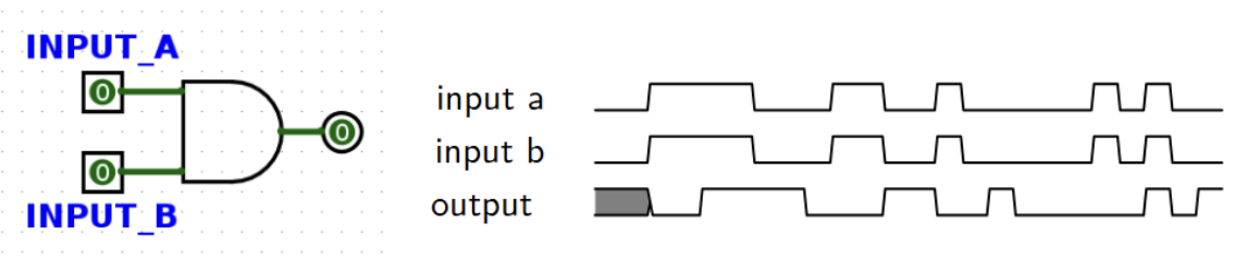
You should notice that the output of this AND gate always changes 2ps after its inputs change. State elements, on the other hand, can remember their inputs even after the inputs change. State elements change value based on a clock signal. A rising edge-triggered register, for example, samples its input at the rising edge of the clock (when the clock signal goes from 0 to 1).
Textbook Readings
P&H A.3-A.6
Additional References
These notes would not be possible without Professor John Wawrzynek’s CS 61C handouts:
Exercises
Check your knowledge!
Conceptual Review
Solution
False. Different gate arrangements that implement the same logic can have different propagation delays, which can affect the allowable clock speed.
Solution
False. A wide circuit with more gates in parallel can have less delay than just a few gates arranged in sequence.
Solution
False. This can result in instability if registers are connected to each other, as register outputs may not have propagated properly before the next rising edge.
Solution
True. NOR can be used to express AND, OR, and NOT gates. Thus, NOR is functionally complete and can be used to represent any possible Boolean expression, and thus any combinational logic circuit.
Solution
False. The minimum clock cycle must allow enough time for every combinational logic delay to settle on an output, so the frequency is based on the longest combinational logic delay possible between state elements.
Short Exercises
Solution
NOT, AND, OR, XOR, NAND, NOR, XNOR
Here are the outputs for each boolean function combined into a single truth table. All possible combinations of the inputs and are shown the left, and the output of the the boolean function based on the current inputs is shown on the right
| Input(s) | NOT | AND | OR | XOR | NAND | NOR | XNOR |
|---|---|---|---|---|---|---|---|
| 0 0 | 1 | 0 | 0 | 0 | 1 | 1 | 1 |
| 0 1 | 1 | 0 | 1 | 1 | 1 | 0 | 0 |
| 1 0 | 0 | 0 | 1 | 1 | 1 | 0 | 0 |
| 1 1 | 0 | 1 | 1 | 0 | 0 | 0 | 1 |