Signals, Waveforms, and the Clock
Learning Outcomes
- Interpret the waveform diagram of the clock signal.
- Identify the propagation delay of a combinational logic circuit.
🎥 Lecture Video
In the previous chapter, we discussed a chip, which is composed of wires and transistors (among other things):
Apple A14 Bionic Chip (sources: Wikipedia, TechInsights. #fig-apple-a14 in Intro to SDS.
Surrounding the inner part of the chip—the core—is a set of connections to the outside world. Usually these connect through some wires in the plastic or ceramic package to the printed circuit board (PCB). In the case of most computers this PCB would be the motherboard. Some of these connections go to the main memory and the system bus. A fair number of the pins are used to connect to the power supply. The power supply takes the 110 Volt AC from the wall socket (provided by PG&E) and converts it to low voltage DC (usually in the range of around 1 to 5 volts, depending on the particular chip used). The DC voltage is measured relative to ground potential (GND). Power connections to the chip from the power supply are of two types; GND, and DC Voltage (labeled “Vdd”).
The energy provided by the power supply drives the operation of the processor. The energy is used to move electric charge from place to place in the circuits and in the process is dissipated as heat. These days a processor my use on the order of 10 watts—like a not-so-bright light bulb.
The Clock
Another special connection to the chip is the clock input signal1. The clock signal is generated on the motherboard and sent to the chip, where it is distributed throughout the processor on internal wires.
If we had a very small probe we could examine the signal on the clock wires, by looking at the voltage level on the wire. We would see a blur, because the clock signal is oscillating at a very high frequency (around 1 billion cycles/second or 1GHz, these days). If we could record it for a brief instant and plot it out we would see something like #fig-clock-waveform.
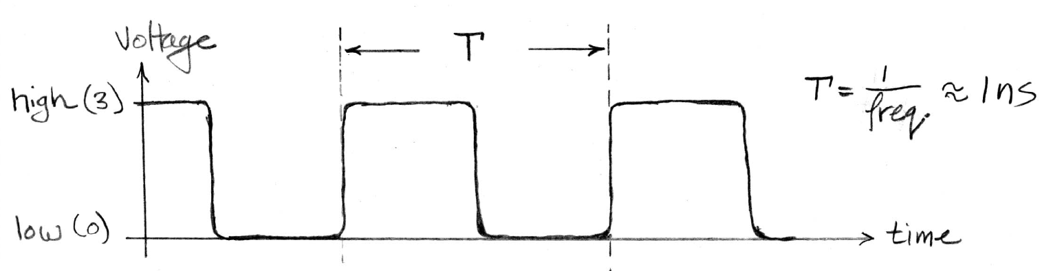
Waveform for a clock signal if recorded and plotted over time.
For CS 61C, we will almost always measure the clock period from the rising-edge of the signal to the next rising-edge. We will see later that the clock signal is a very important signal and is present in all synchronous digital systems.
Why are they called *rising* and *falling* edges of the clock signal?
The idea of rising and falling edges comes from the idea of imagining that the signal might start at a low voltage and rise to the high voltage, stay there for half the period, and then fall to the low voltage, where it stays for another half period, etc.
Signals and Waveforms
Similarly to the clock signal, we can look at other signals in the circuit. For instance, suppose we found an adder circuit. How would we know it’s an adder circuit? We could put a recording probe at its input and observe a waveform1 like #fig-adder-waveform.
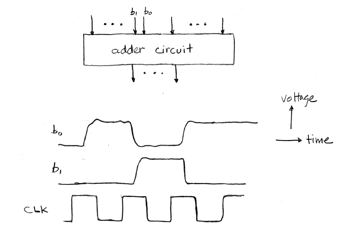
Waveform for signals in an adder circuit if recorded and plotted over time.
If we had two probes, we could look at two signals simultaneously. Imagine that we probe the two least significant bits of one of the inputs to the adder. Based on the recorded waveforms, displayed above the clock signal in #fig-adder-waveform, we can make the following observations.
- Most of the time, the signals are in one of two positions: low voltage or high voltage.
Why?
By convention, low voltage is used to represent a binary 0 and high voltage is used to represent a binary 1. At different points in time, the particular bit position of the input to the adder has a value of 0, and at other times, has a value of 1.
- When the signals are at the high or low voltage levels, they are sometimes not quite all the way to the voltage extremes.
Why?
The transistor circuits that make up the adder and its subcircuits are robust against small errors in voltage. If the signal is close to high voltage, it is interpreted as a logic 1, and similarly, if it is close to 0 volts, it is interpreted as a logic 0. Therefore, errors (or deviations from ideal voltages) do not accumulate as signals move from circuit to circuit.
The circuits have the property that they take input signals that may not be ideal, in the sense of being exactly at the voltage extremes, and produce outputs precisely at the voltage extremes. This restoration property is a critical property of digital circuits!
- Changes in the signals seem to correspond to changes in the clock signal, but they don’t always change every time the clock cycle changes.
Why?
In synchronous systems, all changes follow clock edges. The clock signal is used throughout the system to control when signals may take on new values.
Signal Wires
Signal wires are often grouped together to transmit words of data, as shown in #fig-sig-wires. This drawing shows a collection of 4 wires used to transmit a 4-bit word. The waveforms show how the signals on the wires might change over time. Lower-case letters are used to label the individual wires and signals. The corresponding upper-case letter is used to label the collection of wires (sometimes referred to as a bus). Drawing a single waveform that represents all the signals on the bus is difficult because, at any instant, each wire could have a different value. If we need to show the timing of the changes of the signals on a bus, we can draw a waveform like #fig-sig-wires. Here, we draw the bus signal as simultaneously high and low voltage, and label each closed section with the value on the bus at that instant. In addition to the values on the bus, the timing of the changes is another important piece of information we can observe from waveforms like this.
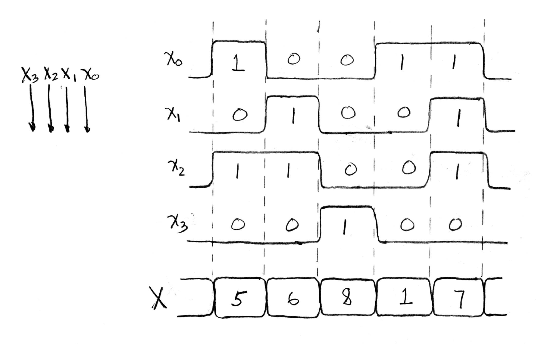
Waveform diagram of signal change over time along 4 wires.
Circuit Delay: Propagation Delay
Summary: Synchronous Digital System
#fig-general-model-sds shows the general model for our synchronous systems:
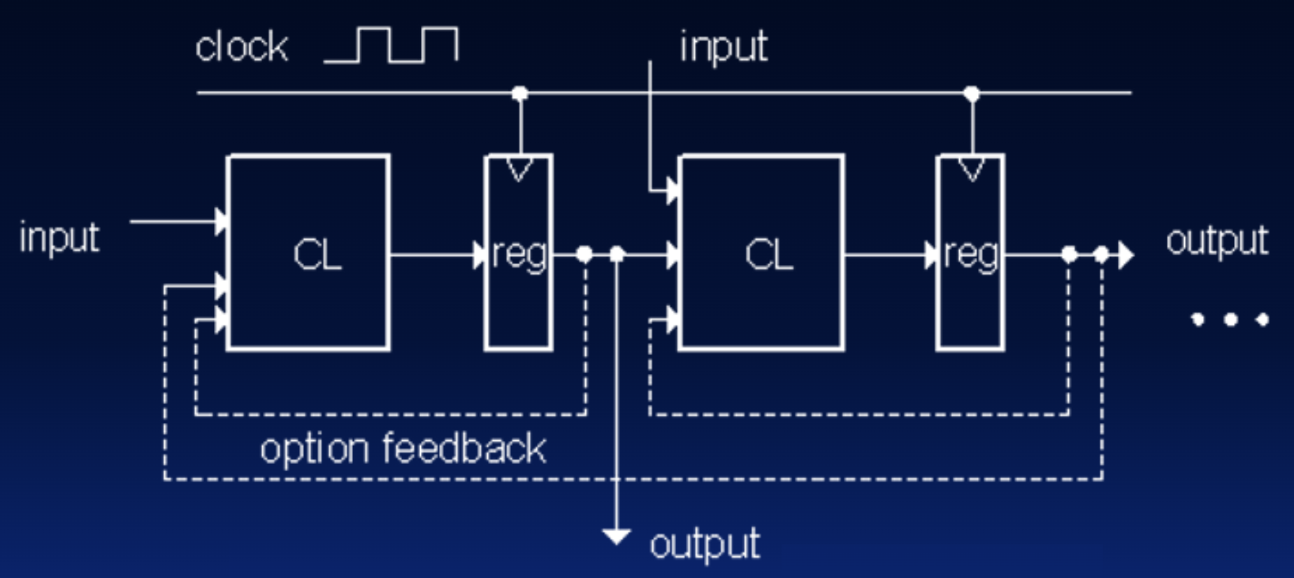
General model for SDS.
- Our circuit is a collection of combinational logic blocks (CL blocks) separated by registers.
- Registers may be back-to-back; CL blocks may be back-to-back.
- Feedback is optional.
- Clock signal(s) connects only to clock input of registers. Combinational logic blocks are stateless and not clocked.
Footnotes
-
These notes are adapted from Professor John Wawrzynek’s notes: SDS Handout. ↩ ↩2