R-Type Datapath, ALU
Learning Outcomes
- Implement a datapath that supports R-Type instructions.
- Compare the datapath elements and logic needed to support
addandsubinstructions. - Reason about the high-level design of an ALU element that supports RV32I instructions.
🎥 Lecture Video
Until 7:40. The add timing from 7:40 onwards is discussed in a later section.
🎥 Lecture Video
Building a processor that adds
To start off, let’s build the simplest processor we can: a processor that can process only one instruction: add. Programs will just be a series of adds:
add x18 x18 x10
add x18 x18 x18
add ...In order to support add in our datapath, we consider the two state elements changed by this instruction’s operations:
- RegFile: We read two registers
rs1andrs2and write one registerrd. The value to write is the sum between the two read register values,R[rs1] + R[rs2]. - PC: We read from and write to the PC register. The value to write is
PC + 4.
Other state elements:
- IMEM: The processor must read the RV32I instruction from the read-only IMEM during the
IF(Instruction Fetch) phase. - DMEM: The processor does not additionally access memory via a load or store. The
addinstruction does not participate in theMEMphase of the five step process.
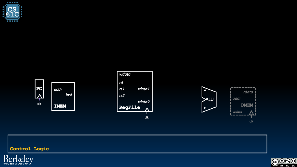
For now, we disconnect DMEM since it is unused for add (@fig-add-no-dmem). We will add it back when we discuss loads and stores.
Tracing the add Datapath
Given the above analysis, we can now connect wires between key elements of our processor.
-
Instruction Fetch:
- On the rising clock edge, the
pcwire updates to the instruction to execute in this cycle. It feeds into IMEM which, after some delay, updates theinstoutput signal. - Increment the PC to the next instruction. The
pcwire also feeds into a small adder that adds4. The output to this small adder is wired to the input of thePCregister, set up and ready to update on the next rising clock edge.
- On the rising clock edge, the
-
Instruction Decode: We only have one instruction, so decoding is simply decoding the specific bits to identify the registers. We use the green card and our R-Type format to introduce a splitter on the
instsignal to “index” into the RegFile as follows:- Wire
inst[7:11](bits 7 through 11, inclusive) to therdinput of RegFile. - Wire
inst[15:19]to thers1input of RegFile. - Wire
inst[20:24]to thers2input of RegFile.
After some delay, the RegFile updates the
rdata1andrdata2signals to the values ofR[rs1]andR[rs2], wherers1andrs2are determined from the instructioninst. - Wire
-
Execute: Our ALU (see below) should perform the Addition operation. For now, we just mark this block as an Adder. Feed in the two RegFile output signals into the
AandBinputs of the “ALU.” After some delay, the -
Memory: (We don’t access memory, so skip this.)
-
Write Back: Connect the output signal of the ALU to the
wdatainput signal of the RegFile. Set the RegFile control signalRegWEnto1to indicate thatwdatashould be written toR[rd]on the next rising clock edge.Around the next rising clock edge,
wdata,RegWEn, andrdshould be held stable through setup and hold time of RegFile.
Building a processor that adds and subs
Next, let’s improve our processor by supporting two instructions: add and sub. Example program:
add x18 x18 x10
sub x18 x18 x18
sub ...
add ...
Let’s again consider the state elements changed by this instruction’s operations:
- RegFile: We still read two registers
rs1andrs2and write one registerrd. But now the value to write is the difference between the two read register values,R[rs1] - R[rs2]. - PC: We read from and write to the PC register. The value to write is
pc + 4.
sub is almost the same as add, except now the ALU subtracts. We implement the support for both add and sub by assuming more complexity in the Control Logic “block” (@fig-sub-datapath).
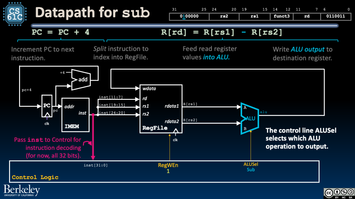
To implement sub and add, we update control logic.
How do we determine add or sub? Recall our discussion of Design Decisions for R-Type: add and sub have the same opcode and funct3 fields, but different funct7 fields. Importantly, the inst[30] bit is 1 for sub and 0 for add.
Building an R-Type processor
We can extend our reasoning above to build a processor that implements all R-Type instructions:
- Build an ALU that supports all R-Type arithmetic and logic operations on operands
R[rs1]andR[rs2]. - Build a Control Logic block that use the instruction bits
instto select the appropriate ALU operations and setALUSelaccordingly.
Arithmetic Logic Unit (ALU)
We encourage revisiting this section after reading a few more example datapath traces.
In the previous chapter we implemented a basic four-operation ALU. As shown in #fig-element-alu and #tab-alu-signals, the RISC-V ALU takes the same input and output, but the control signal ALUSel is much wider to accommodate the functionality needed for the full RISC-V datapath.
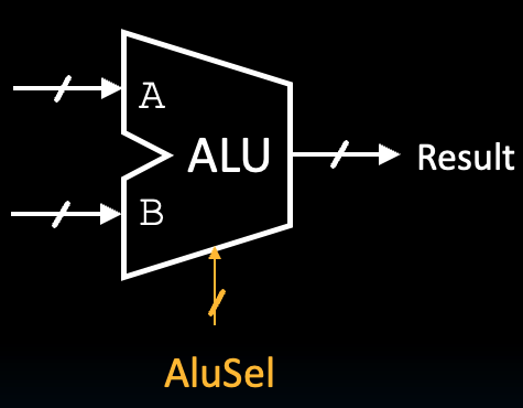
ALU Block.
In the full RISC-V implementation, our ALU (@fig-element-alu) must perform arithmetic for many signals:
- Register-register arithmetic and logical operations for R-Type instructions
- Register-immediate arithmetic and logical operations for I-Type instructions
- Base + Immediate address computation for loads and stores
- PC-relative address computation (See datapath for Branches and Jumps)
- Upper immediate computation (see datapath for U-Type)
Course Project Details
Below, we detail the ALU operations that must be implemented for the course project’s datapath.
Observations/reminders:
- When performing shifts, only the lower 5 bits of
Bare needed, because only shifts of up to 32 are supported. - The comparator component might be useful for implementing instructions that involve comparing inputs. See the branch implementation later in this chapter.
- A multiplexer (MUX) might be useful when deciding between operation outputs (recall our basic 4-operation ALU). Consider first processing the input for all operations first, and then outputting the one of your choice.
- See general multiplication notes below.
General Multiplication
An ALU that implements the mul, mulh, and mulhu instructions can support parts of the RISC-V “M” extension.
| Instruction | Name | Description | Type | Opcode | Funct3 | Funct7 |
|---|---|---|---|---|---|---|
mul rd rs1 rs2 | MULtiply | R[rd] = (R[rs1] * R[rs2])[31:0] | R | 011 0011 | 000 | 000 0001 |
mulh rd rs1 rs2 | MULtiply Higher Bits | R[rd] = (R[rs1] * R[rs2])[63:32] (Signed) | R | 011 0011 | 001 | 000 0001 |
mulhu rd rs1 rs2 | MULtiply Higher Bits (Unsigned) | R[rd] = (R[rs1] * R[rs2])[63:32] (Unigned) | R | 011 0011 | 011 | 000 0001 |
The result of multiplying 2 32-bit numbers can be up to 64 bits of information, but we’re limited to 32-bit data lines, so mulh and mulhu are used to get the upper 32 bits of the product. The Multiplier component has a Carry Out output (with the description “the upper bits of the product”) which might be particularly useful for certain multiply operations.