Instruction Timing
Learning Outcomes
- Practice interpreting waveforms in timing diagrams.
- Given an instruction, identify the critical path through the single-cycle datapath.
- Approximate instruction timing based on the five phases of instruction execution.
🎥 Lecture Video
How should we time our single-cycle datapath? How should we set the clock frequency? In this section, we develop an approximation of instruction timing using the five steps to a RISC-V instruction.
Timing Diagram for add
First, let’s consider the delays in our beloved add instruction. Review the add datapath in #anim-datapath-add-full.
#fig-timing-add shows the waveforms for executing an add x1 x2 x3 instruction at address 0x100, followed by add x6 x7 x9 at address 0x104.
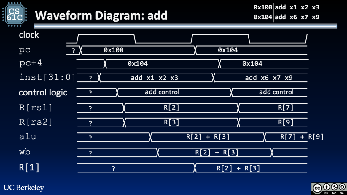
Timing diagram for add. Only relevant signal waveforms are shown.
Critical path delay by instruction
Different instructions use different components of the datapath. We now update our definition of critical path to consider the path between clocked element inputs and outputs that matter for the given instruction. For example, accessing DMEM does not matter for an add, whereas setting up the RegFile data to write back does not matter for sw.
Show Answer for `add`
B. There are two “loops” that we consider:3
- The PC update loop, measured from the PC output to the PC input:
- The loop through the ALU, measured from the PC output to the RegFile input:
The critical path uses the longer loop through the ALU.
Show Answer for `beq`
E. Something else.
We leave this derivation to you. Note you may need to make new placeholder delays for control logic…!
Show Answer for `lw`
C. Load uses hardware in all five phases of the datapath. We still consider the two “loops” through the datapath3:
- The PC update loop, still measured from the PC output to the PC input.
- The much longer loop, measured from the PC output through the ALU and DMEM, to the RegFile input. We now consider additional hardware for loads:
- Instruction Decode: The immediate generation block sets
immconcurrently with the RegFile retrieving the source register valueR[rs1]. We denote this delay as the larger of the two, . - Execute: The ALU output computes the memory address, so we incur .
- Memory: The DMEM read now matters, so we incur DMEM read time, .
- Instruction Decode: The immediate generation block sets
The single-cycle datapath clock is slow
To determine the clock frequency for the single-cycle datapath, we compute delays of each instruction’s critical path, then set the clock period as the worst-case delay incurred over all instructions.
To put some numbers to our earlier analysis, we will simplify our time estimates with #tab-timing-steps, which assumes that the timing of each of the five steps to a RISC-V instruction are dominated by the major functional hardware units.
We can then produce the simplified timing diagram in #fig-timing-phases for an instruction that uses all phases—like our lw instruction from earlier.
We can additionally construct
#tab-timing-instructions, which shows the time required for various instruction formats.
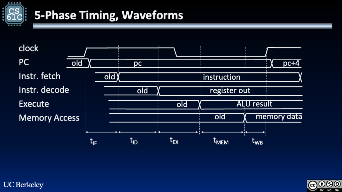
Approximate timing diagram for the five steps to a RISC-V instruction in the single-cycle-datapath.
While #tab-timing-instructions above shows the shortest time to complete each instruction, we note that the single-cycle datapath, like all synchronous digital systems, shares a single clock.
We further note that each instruction’s critical path often involves accessing major hardware units in sequence. In other words, for most of each clock period, much of our hardware is idle and not computing additional data!
We address these performance issues and more in our pipelined datapath design up next. Stay tuned!
Footnotes
-
These processes take a comparable amount of time, though which is longer depends on the specific technology. In #fig-timing-add, the adder happens to complete faster than the
IMEMmemory fetch. ↩ -
Note that the waveform represent bundles of wires with a hexadecimal value (contrast this with the clock’s binary high-low signal). The PC output
pcbundle of wires update at the same time, because flip-flops are wired in parallel. By contrast, thepc+4output does not stabilize simultaneously. Because the adder cascades single-bit adders in series, the least significant bits stabilize sooner than the more significant bits. In timing diagrams, we always show the transition to the correct value. Forpc+4, this occurs after the propagation delay of the most significant bit. ↩ -
In #fig-timing-add, the control logic decoding of the instruction happens to complete faster than the
RegFileregister read. We will assume this precedence in later analysis. ↩ ↩2 ↩3 -
There are two multiplexers controlled with ASel and BSel, respectively. Both propagation delays occur concurrently, so we only count for one mux’s propagation delay. ↩