Adder/Subtractor
Learning Outcomes
- Implement an n-bit adder as a cascade of 1-bit adders.
- Recall that XOR is a conditional inverter and can be used with SUB to augment the adder block into an adder/subtractor block.
🎥 Lecture Video
#fig-add-sub-block shows the add/subtract block used in our basic ALU:
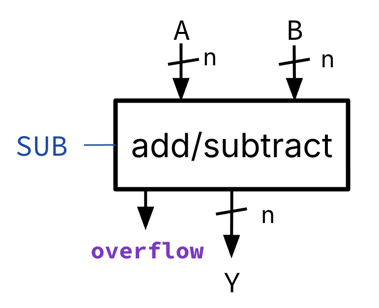
Adder/Subtractor block.
This single circuit is capable of addition and subtraction:
- two 32-bit wide data inputs
AandB - a 1-bit wide control input
SUB. - a 32-bit wide data output
Y - a 1-bit wide output
overflow.
When SUB=1, the circuit performs the subtraction A - B. When SUB=0 the circuit performs the addition A + B.
The “special” output, labeled overflow signals for integer overflow. Upon performing an addition or subtraction, this output will be a 1 if the result is too large to fit in 32 bits. We return to this fact later.
To design our adder/subtractor circuit, we will start out by studying the design of an adder circuit, then later augment it to also perform subtraction.
Cascading Intuition
One strawman1 method for arriving at the detailed gate-level circuit for the adder would be to follow the procedure we learned in the previous chapter2. Unfortunately, that technique is only effective for very narrow adders (e.g., 1-bit or 2-bit wide), because the size of the truth table is too large for wider adders.
Therefore, we turn to modular design: Find a way to break the design up into smaller more manageable pieces. We will design the smaller pieces individually, then wire them together to create the entire wide adder.
Consider adding two 4-bit numbers A= a{sub}3a{sub}2a{sub}1a{sub}0 and B= b{sub}3b{sub}2b{sub}1b{sub}0:
Example, where A is 1011 and B is 0001:
1-bit Adder
Addition in the i{sup}th spot produces two outputs:
- Result bit, i.e., y{sub}
i - Carry bit (e.g., c{sub}
i+1which feeds into the addition in the (i+1){sup}thspot addition. We name a carry bit according to the stage to which it is an input.
Zero-th spot
We build our intuition for implementing a 1-bit adder by considering the adder in the zero-th spot (least significant stage). This computes the least significant result bit, , and the carry-out bit of the least significant stage, .
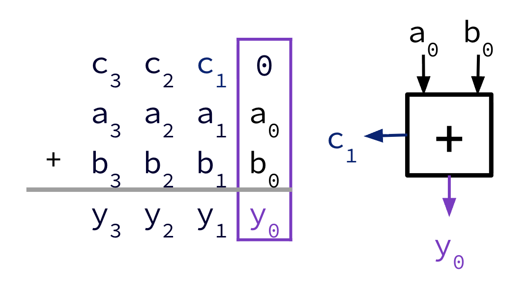
1-bit adder in zero-th spot, without carry-in bit.
By inspection of the truth table in #tab-adder-1-zero, we can directly write the logic equations for this stage3.
First spot
Next, consider the logic for the next significant stage (and all subsequent stages):
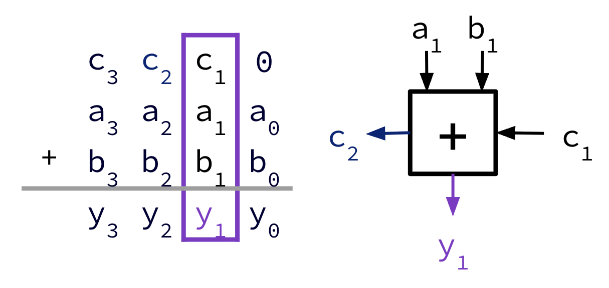
1-bit adder in first spot, with carry-in bit.
Even though the truth table is larger, the logic equations are still straightforward to write—at least, if we remember what we learned from previous sections.
Why does the truth table have 8 rows?
The truth table now has 8 rows, because there are three inputs into this stage:
- a bit from each of A and B, along with
- the carry-in bit for this current stage, which is also the carry-out from the previous stage.
Why XOR for result bit, and MAJ (Majority) for carry bit?
By carefully inspecting the truth-table you will notice:
- Result bit : The sum output is the XOR of the three inputs. Recall that an N-bit XOR is a 1 when the number of 1’s in the input is odd.
- Carry-out bit : The carry-out function is the majority function. Recall that a 3-way majority circuit is a 1 when the number of 1’s in its input is greater than the number of 0
General case
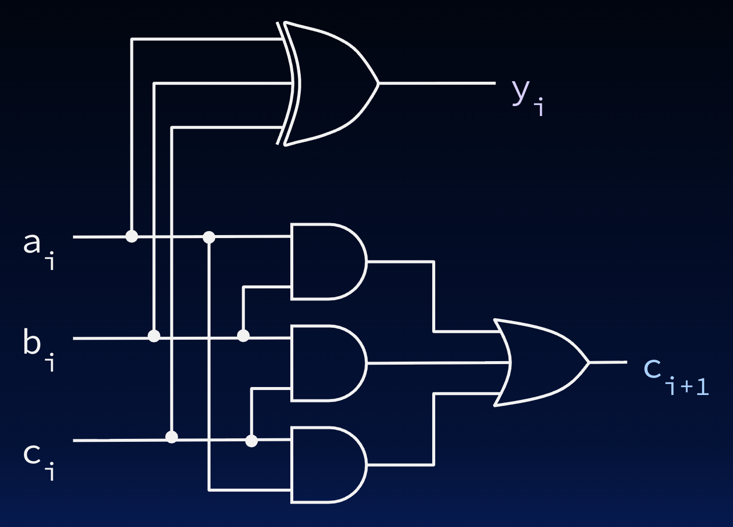
Let us finally consider the logic for the i{sup}th spot, where for an -bit wide addition. We will encapsulate the operations of one stage, or column, of the add operation into a small block, shown in #fig-adder-1-i:
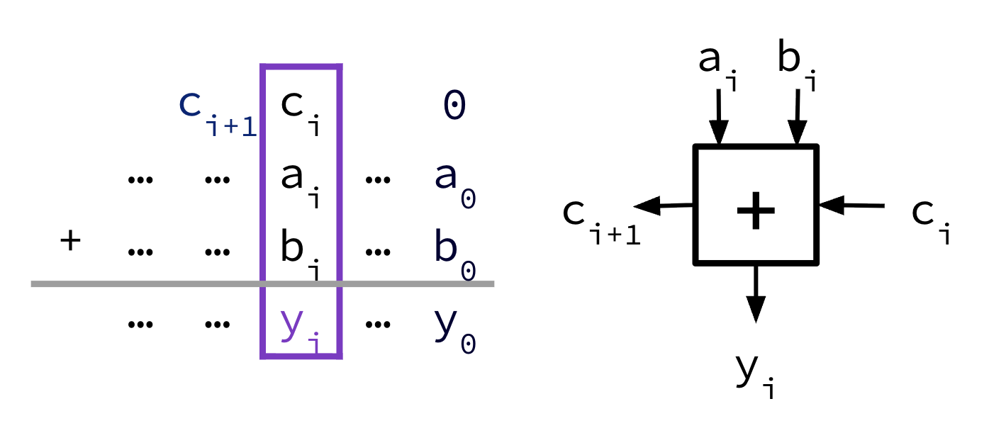
1-bit adder in i{sup}th spot, with carry-in bit.
You can think of this block as a 1-bit adder. It’s official name is a full-adder cell, but most people confuse this with an n-bit adder, which it certainly is not.
The 1-bit adder’s gate-level circuit diagrams for its internals are in #fig-adder-1-i-circuit. The logic equation can be pattern-matched from our earlier discussion and is Equation #eq-adder-1-i.
N-bit Adder
The next step in the design of our adder circuit is to wire together a collection of our 1-bit adders to create an n-bit adder. All we need to do is to wire the carry-out output of one stage into the carry-in input of the next, from least significant to most, as shown in #fig-cascade-add:
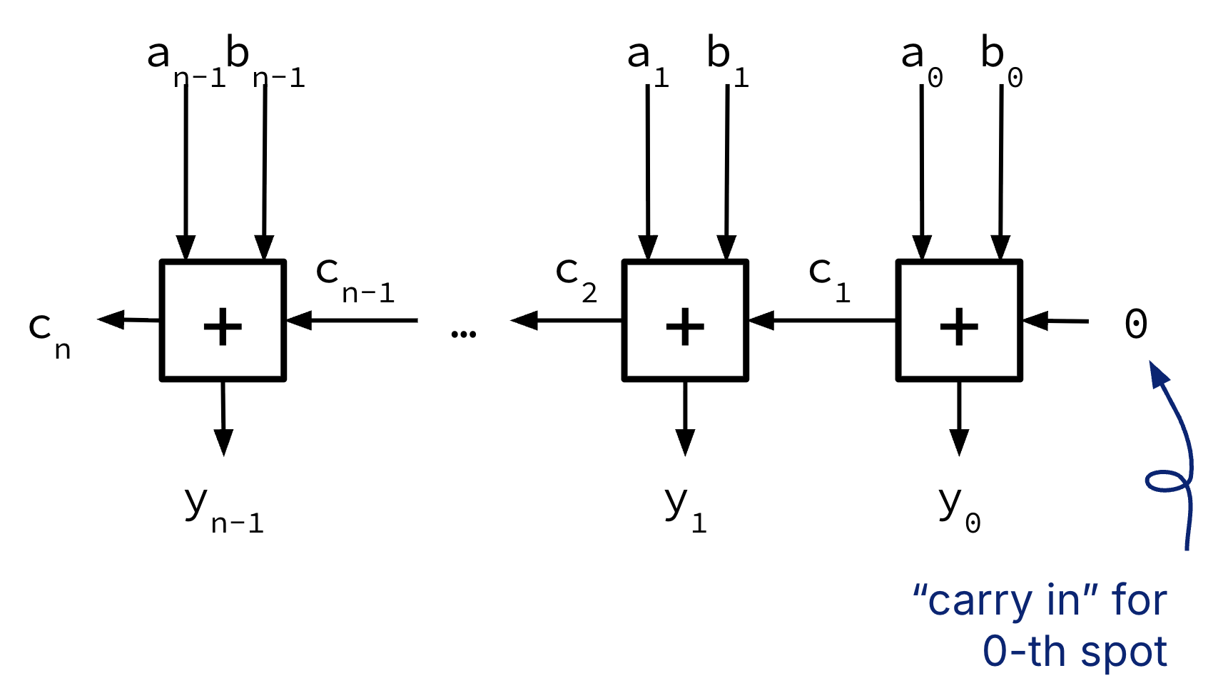
(Incomplete) Cascading n-bit adder. The carry-in bit c{sub}0 is set to GND, but the carry-out bit c{sub}n is currently unused.
Inputs are applied at the top and after some delay, associated with the delay through the logic gates for the blocks, and the delay of the carry from stage to stage, the final result appears at the bottom.
What to do with carry-in bit c{sub}0? For the adder to produce the correct result, convince yourself that c{sub}0 must be connected to a source of logic 0 (GND in the circuit). But we will find something more interesting to do for c{sub}0 when we discuss the subtractor below.
What to do with carry-out bit c{sub}n? The carry-out from the most significant stage, c{sub}n, can be used as the (n+1){sup}th bit of the result (remember, adding two n-bit numbers could result in a (n+1)-bit result). However, in most uses for an adder, we must generate an n bit result. For instance, RV32I registers can only store 32 bits, so the result of the add instruction must be a 32-bit number. In this case, we must signal overflow, which we discuss next.
Overflow
As discussed in our initial adder/subtractor design, an overflow output must be generated to indicate when the result cannot fit into n bits. Recall from an earlier section that overflow can occur when adding a pair of negative numbers or when adding a pair of positive numbers.
We can make the following observations about adds in this circuit. Remember, the most significant stage is the stage associated with the sign bit, i.e., stage n-1.
- If there was a carry in to the most significant stage, but no carry out of that stage, then A and B were both positive and the result of the addition overflowed, erroneously generating a 1 in the sign bit position.
- If there was a carry out of the most significant stage and no carry out that stage, then A and B were both negative and the result of addition overflowed.
- In all other cases the value of the carry in to the most significant stage matches the carry out, then there was no overflow.
We demonstrate this intuition in #fig-2bit-add-overflow-table for a 2-bit adder.
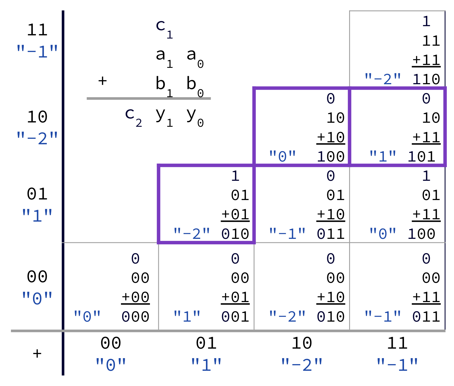
2-bit adder overflow table diagram. Overflow occurs when adding , , and . Notably, the first is a valid addition, where the latter two produce incorrect results.
Show Explanation of [#fig-2bit-add-overflow-table](#fig-2bit-add-overflow-table)
#fig-2bit-add-overflow-overview provides a high-level idea of addition with 2-bit numbers A and B. Keep the integer wheel on the left in mind when adding integers. Keep the integer wheel in mind when adding integers.
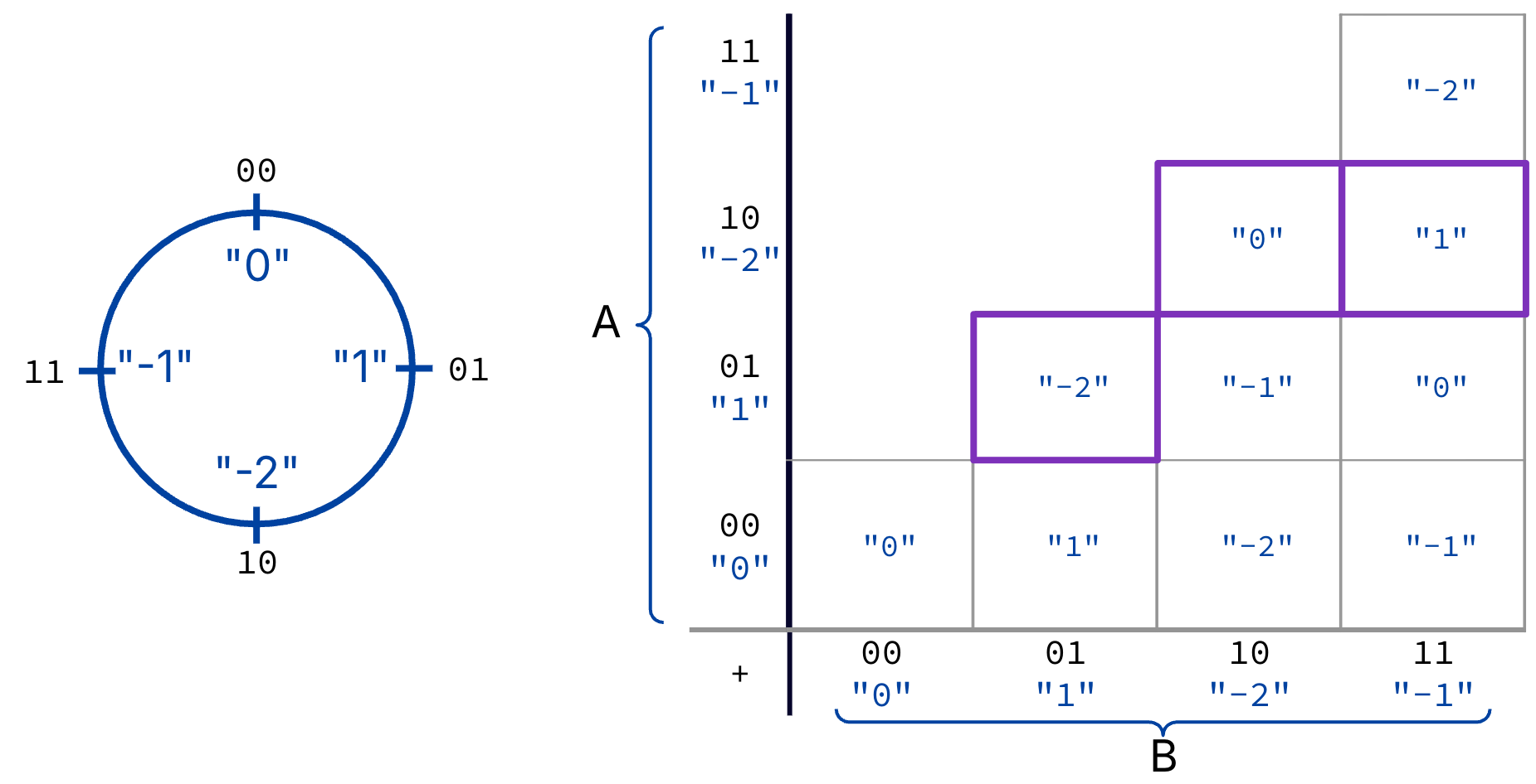
High-level 2-bit adder overflow table diagram.
Three overflow results are boxed in #fig-2bit-add-overflow-table:
- , not
- , not
- , not
The original #fig-2bit-add-overflow-table shows the bit patterns of these three additions (among others), resulting in the three observations in this section.
Based on these observations, we can design a simple circuit that generates the overflow output signal by comparing the carry-in and carry-out of stage n-1. A simple circuit that indicates when two signals are different in value is the XOR gate.
#fig-cascade-add-overflow shows our full n-bit adder:
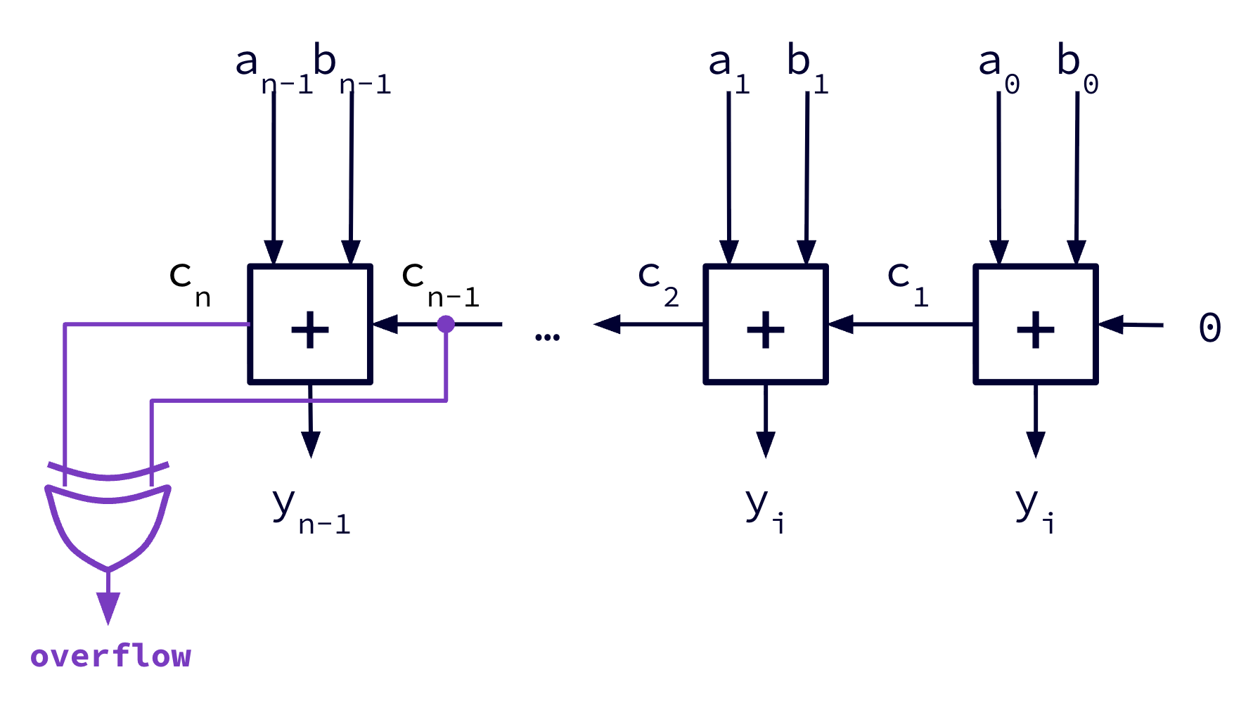
Cascading n-bit adder with overflow.
Subtractor
We mentioned earlier that addition and subtraction are closely related, and therefore we would expect that their respective circuits are similar and could serve dual both purposes.
As discussed in our initial adder/subtractor design, a control bit SUB signals if the add/subtract block should perform subtraction. We note the following holds, due to two’s complement:
- When SUB=0 the circuit performs the addition
A + B. - When SUB=1, the circuit performs the subtraction
A - B. The following statements are erquivalent:- Compute
A + (-B), whereBis the two’s complement. - Compute
A + ~B + 1. This is the definition of two’s complement: invert bits and add 1.
- Compute
This last observation gives us a very clean way to augment our adder circuit to be a combined adder and subtractor:
- Add 1 to the result.
- Invert the bits of
B.
The augmented adder design is shown below. When the input SUB is 1 the block performs subtraction, when SUB=0 the block performs addition.
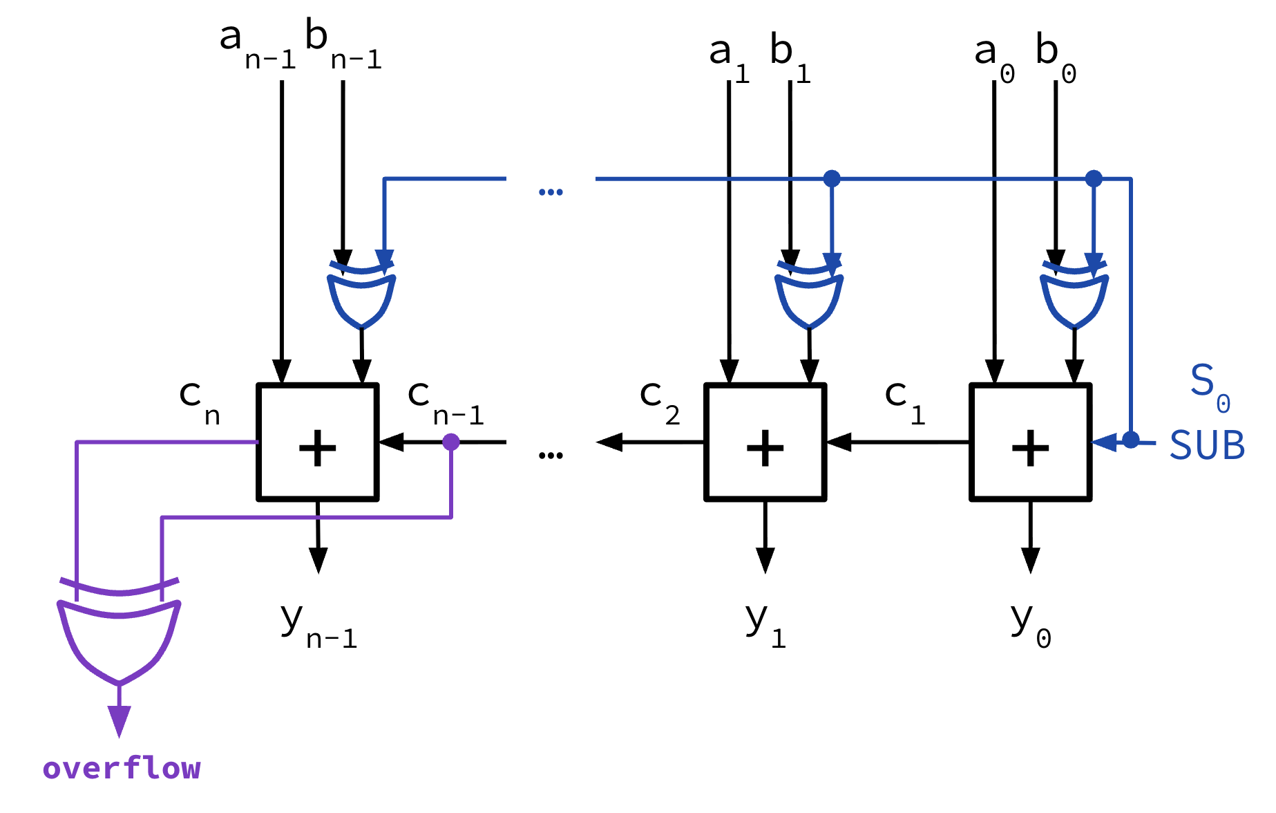
N-bit adder/substractor design circuit diagram.
Footnotes
-
As discussed in the previous chapter: Start with a truth table, write the canonical Boolean equation, then simplify. ↩
-
^: XOR,&: AND ↩