State Elements on the Datapath
Learning Outcomes
- Describe the main state elements on the single-cycle RISC-V datapath.
- Identify when data is written on synchronous state elements on the RISC-V datapath.
- Compare and contrast read and write behaviors of RISC-V state elements.
🎥 Lecture Video
As mentioned in the previous section, a CPU has two types of elements, reflecting the design of many digital logic systems.
- State elements that contain state: registers and memory
- Combinational Logic Blocks that operate on data values: ALU, other combinational logic, etc.
In this section, we discuss the state elements needed in a RISC-V processor. We will discuss and introduce the combinational logic blocks as we build out the full datapath.
Program Counter
The Program Counter (PC) is a 32-bit register in #fig-element-pc and holds the value of the current instruction, i.e., instruction to execute in the current clock cycle.
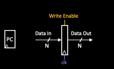
The Program Counter, PC, is a single 32-bit register in the CPU.
PC Signals
Input:
- Data: N-bit data input bus
- Control: Write Enable bit. 1: asserted/high, 0: deasserted/low.
- Clock signal.
Output:
- Data: N-bit data output bus
Behavior:
- Read: At all other times, Data Out will not change; it will output its current value.
- Write: Rising-edge triggered. On rising clock edge, if Write Enable is 1, set Data Out to Data In (delay of clk-to-q).
Register File (Regfile)
The Register File (or RegFile) has 32 registers: register numbers x0 to x31.
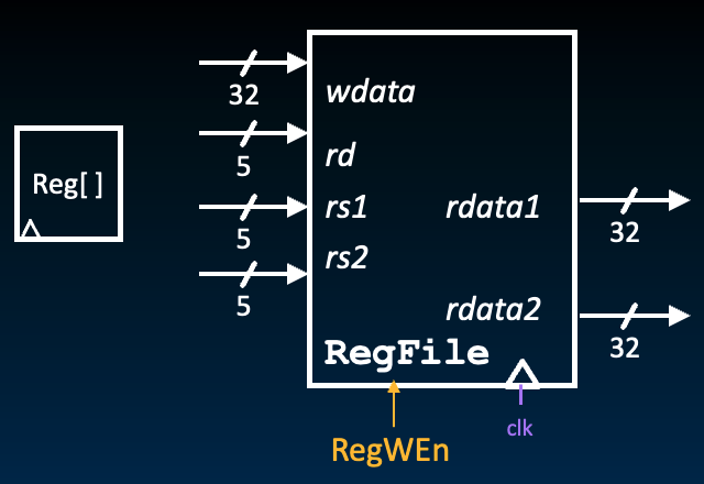
The RegFile is symbolically written as RegFile and is composed of registers x0 to x31.
Behavior:
- Registers are accessed via their 5-bit register numbers:
R[rs1]:rs1selects register to put onrdata1bus out.R[rs2]:rs2selects register to put onrdata2bus out.R[rd]:rdselects register to be written viawdatawhenRegWEnis set to 1.
- Read: As long as
rs1andrs2are valid, thenrdata1andrdata2are valid after access time, regardless of whatRegWEnis set to. - Write: Rising-edge-triggered write. On rising clock edge, if
RegWEnis set to 1, writewdatatoR[rd].
DMEM: Data Memory
For this class, memory is “magic.” Assume a 32-bit byte-addressed memory space, and memory access occurs with 32-bit words. We go into more detail with our course projects.
For our single-cycle datapath, we must access memory twice: once during IF (Instruction Fetch) to read the instruction from memory, and once during MEM (Memory Access) if we load/store data from/to memory. We therefore need two memory blocks: IMEM and DMEM for instruction memory and data memory, respectively.1
The Data Memory block DMEM has edge-triggered writes, just like RegFile.
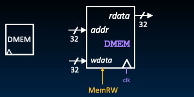
The Data Memory block DMEM. Read operations behave like combinational logic, whereas write operations occur on the rising clock edge.
Behavior: DMEM read/writes behave similarly to Regfile, though now we provide memory addresses as input, not register numbers.
- Read: Address
addrselects word to put onrdatabus. IfMemRWis 0 andaddris valid, thenrdatais valid after access time. - Write: Rising-edge-triggered write. On rising clock edge, if
MemRWis set to 1, writewdatato addressaddr.
IMEM: Instruction Memory
The Instruction Memory block IMEM is a read-only memory that fetches instructions.2
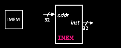
In our CPU, the Instruction Memory block IMEM is read-only and behaves like combinational logic.
Behavior:
- Read: Address
addrselects word to put oninstbus. Ifaddris valid, theninstis valid after access time.
Footnotes
-
Under the hood, IMEM and DMEM are placeholders for L1 caches:
L1i,L1d. See a later section. ↩ -
We will need to write the instruction memory when we load the program, which we ignore for simplicity. ↩