Elements of Architecture: Processor, Registers, and Memory
Learning Outcomes
- Understand that registers are extremely tiny, fast storage located within a processor. In the conceptual layout of a computer, the processor and memory are separately located.
🎥 Lecture Video
🎥 Lecture Video - Memory Hierarchy
Until 5:00
Conceptual Layout of a Computer
In order to learn an ISA, we must first understand #fig-von-neumann, which shows a conceptual layout of a computer:
- A processor (e.g., a Central Processing Unit, or CPU), responsible for computing. Inside the processor, there is a control unit and a data path. The main elements of the data path are the registers and the execution unit, typically called the Arithmetic Logic Unit (ALU). We will discuss all these details soon.
- Main memory, responsible for long-term data storage.
- I/O Devices, i.e., Input/Output Devices like keyboards, displays, etc.
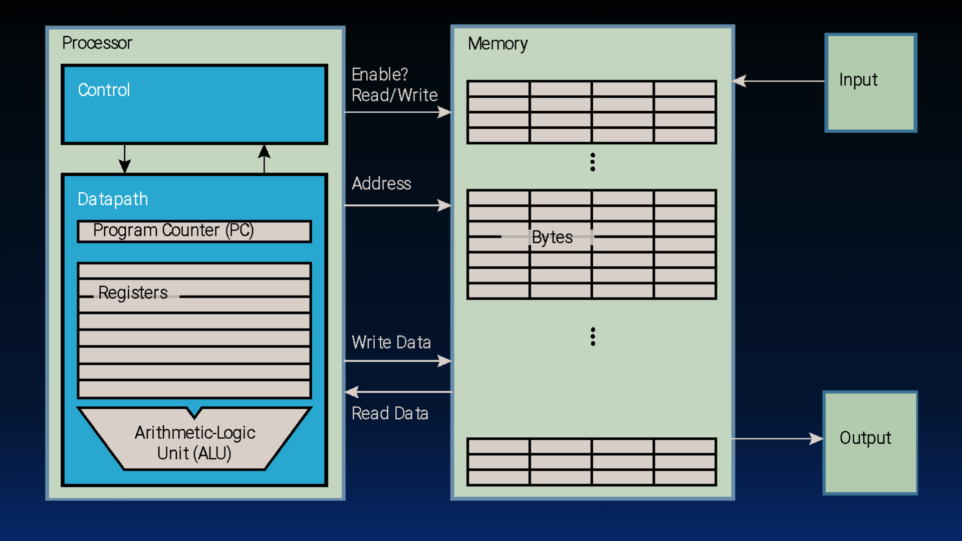
Basic computer layout (See: von Neumann architecture).
Registers
Importantly, the processor is designed to be fast. Four example, if a processor runs at 4 GHz, then it can execute instructions on some data once per cycle, or every 0.25 ns (nanoseconds). This data must also be physically located close to the processor!
Consider that the speed of light (approximately m/s), which physically defines the fastest speed with which to access data from a certain physical location. In other words, accessing something about 10 cm away will already take 0.3 ns (thankfully most of our integrated chips are much smaller than this distance). Nevertheless, in all modern architectures we have at least two pieces of hardware for data:
- Registers, located within the processor itself. These hardware objects have limited space1 are lightning fast; a processor performs operation on these data using the arithmetic logic unit.
- Memory, which is much larger2 and located external to the processor. Memory access is often assumed to take approximately 100 ns (@fig-3-locality). The processor communicates with memory by issuing addresses to read or write data. The “enable” signal additionally ensures we don’t accidentally alter memory values when we only intend to read; we discuss this more later.
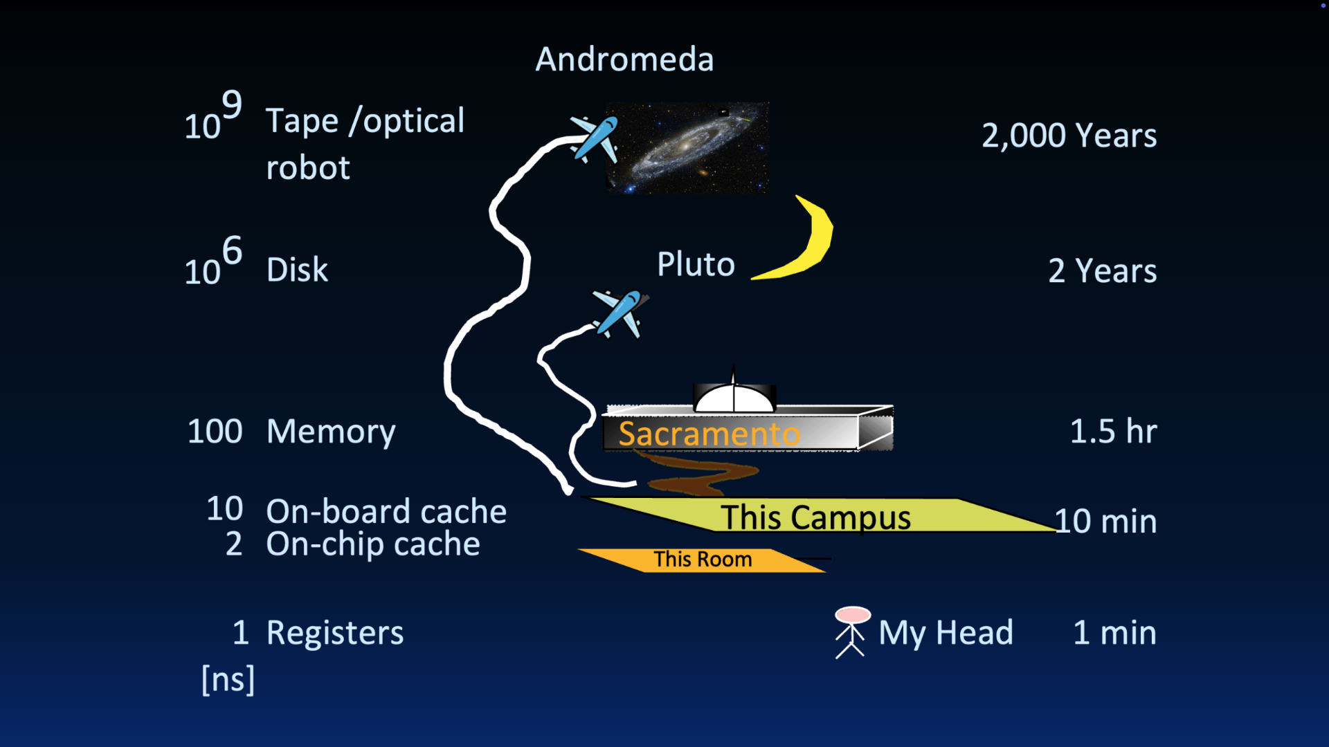
Great Idea 3: The Principle of Locality / Memory Hierarchy
Memory Hierarchy
Each ISA specifies a predetermined number of hardware registers, defining how each of the registers should be used for instruction execution. RISC-V defines 32 registers; read more in the next section.
Remember the picture of the principal memory hierarchy in (@fig-3-memory-hierarchy):
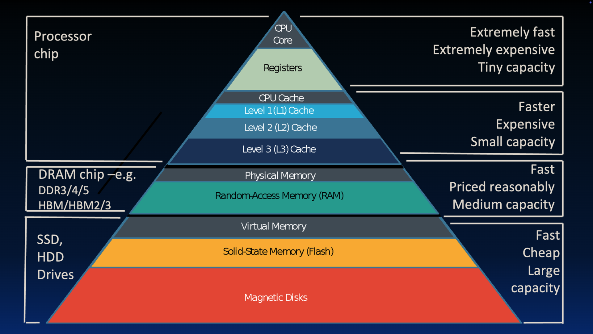
Great Idea 3: The Principle of Locality / Memory Hierarchy
At the very top, we have the processor core with its registers. On a separate chip, we typically have the main memory, implemented using DRAM (Dynamic Random Access Memory). You might have heard of flavors like DDR3, 4, or 5, or High Bandwidth Memory (HBM). While DRAM is fast, it is not nearly as fast as registers. At a reasonable price point, you can get many gigabytes for a few tens of dollars, providing medium capacity.
Physics dictates that smaller is faster. How big is the gap between registers and memory? While a processor has only about 128 bytes of total register storage, a laptop might have 2 to 64 gigabytes of DRAM, and a server might have a terabyte. On the other hand, if we think in terms of latency, registers are about 50 to 500 times faster than DRAM.
Let’s go back to Jim Gray’s storage latency analogy3 in #fig-3-locality. Put another way–if retrieving data from a register in your head takes one minute, retrieving data from memory (which is 100x slower) would be like driving to Sacramento to get a piece of paper you forgot. If the gap is 500x, that’s like driving to Los Angeles and back. That is a massive penalty just to retrieve one isolated data item!
We only have a small number of registers–they are extremely fast and share precious real estate with the processor core, making them extremely expensive. Designing an ISA (and an associated architecture) therefore involves a careful (?) tango (?) of performing operations on data in registers where possible, and spacing out limited but hefty trips to memory and disk. We revisit this careful tango in a later section.