Supporting Loads and Stores
Learning Outcomes
- Implement a datapath that supports loads (I-Type) and stores (S-Type).
- Explain why certain control signals can be marked as “don’t care” (*).
- Implement partial loads and stores for the course project, and gain a basic understanding of the minimum requirements for the DMEM block.
🎥 Lecture Video
🎥 Lecture Video
Building a Processor with DMEM access
Loads and stores participate in the MEM phase of the five step process. We therefore introduce additional logic connecting DMEM to the ALU and the RegFile. #fig-lw-new-blocks describes DMEM access for load instructions.
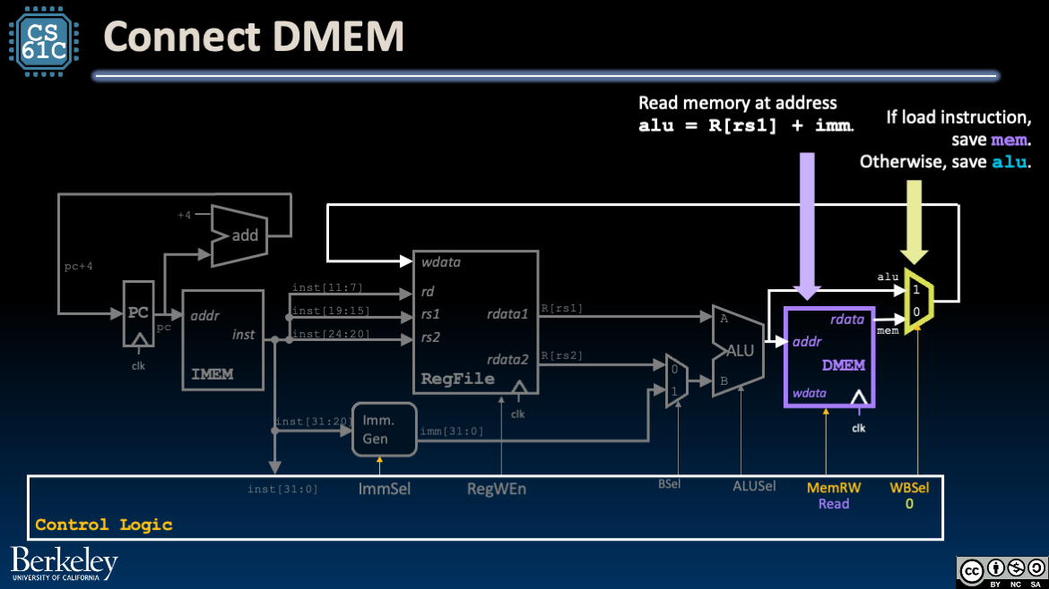
For the MEM phase of a load instruction, conect DMEM to the ALU and use a mux before WB (Write Back) phase.
DMEM: To read the memory at an address, we use the ALU to compute the address as alu = R[rs1] + imm. This readily reuses the circuitry for arithmetic and logical I-Type instructions.
Mux: We now include a mux after the ALU and DMEM that uses the control signal WBSel to select between two values for wdata (the data to write to R[rd]):
- Arithmetic and Logical R-Type or I-Type instructions: The output of the ALU (
alu), which is now wired both intoaddrand into the new mux. - Load instructions: The output of DMEM (
mem).
Tracing the Load Datapath
Recall that load instructions are I-Type because they read a register, have an immediate, and write to a register a 32-bit value read from memory.
For lw, we use a similar datapath to addi, but we use the ALU to compute an address to pass into DMEM. State updates:
- RegFile: We read one register
rs1and write one registerrd. The value to write is a word (again,lw) that is read from memory. - PC: We read from and write to PC. The value to write is
pc + 4. - DMEM: We read the memory word at address
R[rs1] + imm.
-
Instruction Fetch: Increment PC to next instruction (see R-Type datapath). Read the instruction
instfrom IMEM. -
Instruction Decode: Fetch
R[rs1]from RegFile, build the immediateimmfor I-Type instructions (see I-Type datapath). Also configure control logic:- Configure
ImmSeltoI-type immediates. - Set
RegWEnto1. - Set
BSelto1. - Set
ALUSeltoAdd. - Set
MemRWtoRead. - Set
WBSelto0.
After some delay, the immediate generator block updates its output signal
immto the appropriate sign-extended 32-bit immediate value, register valueR[rs1]is read, and control signals are set. - Configure
-
Execute: Because the control line
BSel=1selects the generated immediateimmfor ALU inputB, our ALU computesR[rs1] + imm. -
Memory: Read memory at address
alu = R[rs1] + imm. After some delay, the output signalmemhas the valueMem[R[rs1] + imm]. -
Write Back: Write DMEM output to the destination register and connect the output of the
WBSelmux to RegFile’swdatainput.Around the next rising clock edge,
wdata,RegWEn, andrdshould be held stable through setup and hold time of RegFile.
Tracing the Store Datapath
By contrast, store instructions, by contrast, are S-Type because they read two registers, have an immediate, and write to memory. Stores do not write data to registers.
We do not need to add additional blocks for stores, but we will need to:
- Upgrade the Immediate Generator to support immediates in S-Type instructions; we encourage you to read that section afterwards.
- Wire
R[rs2]towdata(DMEM input signal).
-
Instruction Fetch: Increment PC to next instruction (see R-Type datapath).
-
Instruction Decode: Fetch
R[rs1]andR[rs2]from RegFile, and build the immediateimmfor S-Type instructions. Also configure control logic (see below). -
Execute: Because the control line
BSel=1selects the generated immediateimmfor ALU inputB, our ALU computesR[rs1] + imm. -
Memory: Write memory at address
alu = R[rs1] + immby holdingaddrandwdata(DMEM input).Around the next rising clock edge,
wdata(DMEM input),MemRW, andaddrshould be held stable through setup and hold time of RegFile. -
Write Back: (We don’t write to RegFile, so skip this.)
Partial Loads and Stores: Course project details
This section discusses how to implement partial loads and stores. The details in this section are specific to the course project. We start by introducing additional functions of the course project’s DMEM block.
Recall from an earlier section that according to the RISC-V standard, loads and stores of words should specify word-aligned addresses. DMEM memory accesses in this course (and in the course project) therefore follow the following conventions:
- All DMEM memory accesses are word accesses. Addresses must be 32-bits wide and a multiple of 4.
- Loads read a word (4 bytes) at a time.
- Stores write at most 4 bytes at a time, specified by a bitmask.
Consider #fig-aligned-memory, which shows each byte in memory, referred to by its 32-bit address.
- In a single access, DMEM can access a set of 4 bytes in one of the red boxes in the diagram, e.g., bytes at memory addresses
0-1-2-3or12-13-14-15. - In a single access, DMEM cannot access a set of 4 bytes across two red boxes in the diagram, e.g., bytes at memory addresses
13-14-15-16. This would take two accesses.
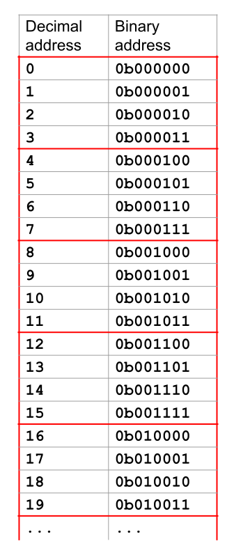
Diagram of aligned memory (Red boxes around every 4 bytes).
Word-aligned DMEM
-
DMEM forces memory accesses to be with addresses of multiples of 4 bytes. DMEM always zeros out the bottom 2 bits of any address you provide (i.e., round down to the nearest multiple of 4), and then accesses 4 bytes starting at this modified address.
For example, if you give DMEM the address
19=0b010011, DMEM will zero out the bottom 2 bits to get16=0b010000, and then start at this modified address to access 4 bytes (16-17-18-19).You don’t need to zero out the bottom 2 bits yourself—the provided DMEM implementation will automatically do this for any address you provide.
-
Assume memory accesses in instructions do not cross word boundaries. All instructions should follow RV32I standard convention and will not cross a word boundary in memory (i.e., a single access will never cross a red line in #fig-aligned-memory).
-
DMEM uses only the lower 16 bits. Due to Logisim size limitations, the memory unit only uses the lower 16 bits of the provided address, discarding the upper 16 bits. This means that the memory can only store bytes of data.
The provided tests will always set the upper 16 bits of addresses to 0, and any tests you write should avoid using the upper 16 bits when interacting with memory.
-
Partial Stores: See the section below for partial-store-specific details, e.g., unit tests.
Partial Load
The partial_load.circ circuit in the course project is designed to take the 32 bits of data read from DMEM, extract the relevant data, then process the data to put into a 32-bit register. The signals for this subcircuit are in #tab-partial-load.
Behavior: For loads, DMEM will always read 32 bits of memory starting at an address that is a multiple of 4 bytes. The partial load subcircuit then uses the instruction itself to determine what bytes to extract.
Example 1. Suppose we had a lb instruction on address 6 = 0b000110.
- DMEM will read the 4 bytes at addresses
4-5-6-7. - We want just the byte at address
6(again, albinstruction). - The bottom 2 bits of the address
6are0b10, so we want the 2nd byte (zero-indexed, i.e., bits 16-23) of the data read from DMEM.
Example 2. Suppose we had a lh instruction on address 9 = 0b001001.
- DMEM will read the 4 bytes at addresses
8-9-10-11. - We want the two bytes at addresses
9-10(again, alhinstruction). - The bottom 2 bits of the address
9are0b01, so we want to start extracting at the 1st byte (zero-indexed) and extract two bytes, i.e., bits 8-23 of the data read from DMEM.
Partial Store
The partial_store.circ circuit in the course project is designed to take data from a register, process it, and store the relevant bytes to memory. The signals for this subcircuit are in #tab-partial-store.
Behavior: For stores, DMEM will write bitmasked data to memory at an address that is a multiple of 4 bytes. Each bit in the 4-bit write-mask MemWriteMask corresponds to the 4 bytes of the word; if a bit in MemWriteMask is 0, DMEM will not store the corresponding byte of DataToMem to memory.
Example 1: Suppose we had a sb instruction on address 3 = 0b000011.
- Of the word’s byte addresses
0-1-2-3, we actually want to just write one byte at address3, because the bottom 2 bits of the address3are0b11(and it is ansbinstruction). - Make a 32-bit value where bits 24-31 are the 8 bits we want to store to memory.3
- Make a 4-bit writemask
0b1000, which says to only write the third byte to memory, leaving the other bytes in the memory word unchanged.
Example 2: Suppose we had a sh instruction on address 2 = 0b000010.
- Of the word’s byte addresses
0-1-2-3, we actually want to write two bytes at addresses2and3, because the bottom 2 bits of the address2are0b10(and it is ansbinstruction). - Make a 32-bit value where bits 16-31 are the 16 bits we want to store to memory.3
- Make a 4-bit writemask
0b1100, which says to only write the second and third bytes to memory, leaving the other bytes in the memory word unchanged.
Note that sh and sb instructions specify data as the lower bits of a 32-bit value, i.e., bottom 16 bits and bottom 8 bits, respectively. See #tab-partial-store-details.
Tips/reminders for the course project:
- Recall that we should not write when our instruction is not a store. When
MemWEncontrol signal is 0,MemWriteMaskshould be set to0b0000. - The bytes in
DataToMemthat aren’t being written to the file (i.e. whereMemWriteMaskis 0) can technically be any value3, but #tab-partial-store-details lists them as 0s in the table. The unit test for this part also assumes that those bytes will be 0.
Footnotes
-
We leave it to you to determine why these cases would/would not cross 32-bit word boundaries. ↩ ↩2
-
Important: The bottom two bits of the
MemAddressaddress (e.g., computed from the instruction) are NOT zeroed. However, DMEM will convert the address to a multiple of 4 before accessing memory. ↩ ↩2 ↩3 ↩4 -
The lower bits 0-23 can be all zeros, though in practice these bits don’t matter beacuse of
MemWriteMask. ↩ ↩2 ↩3