Introduction
Learning Outcomes
- Identify the five steps to executing a RISC-V instruction.
- Explain that the processor datapath describes the flow of data between state elements of the processor.
- Explain that the processor control describes the signals needed to ensure the datapath operations correctly execute the instructions.
🎥 Lecture Video
In this chapter, we will design a RISC-V processor and connect the software and hardware parts of our CS 61C story. In the below figure, this chapter designs the hardware that can actually execute RISC-V code.
Great Idea #1: Abstraction.
There are many such variations of RISC-V processor hardware; we will discuss one such processor this chapter, and a second one soon. There are many other designs of RISC-V chips on the market1. Ultimately, all RISC-V processors must correctly execute RISC-V instructions. Let’s see how!
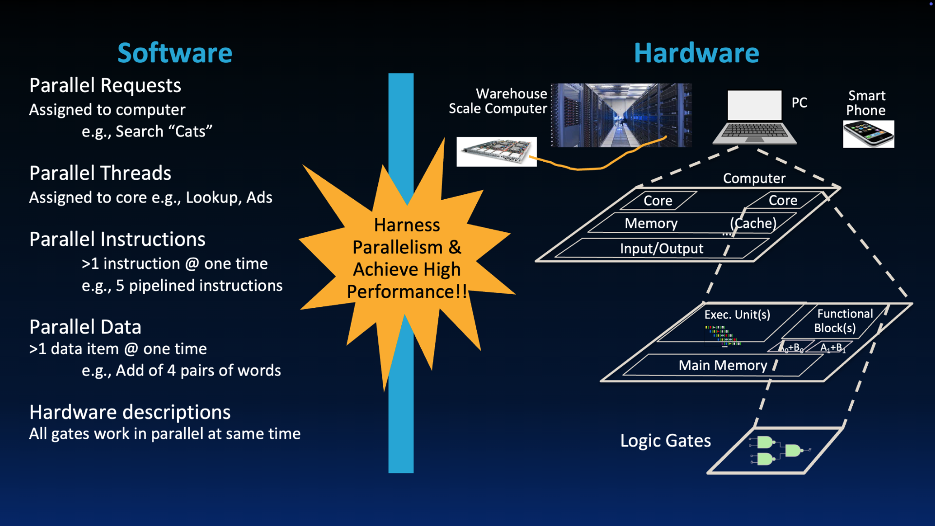
“New-School” Machine Structures leverage parallelism in both software and hardware.
If we execute a single instruction on a single clock cycle, combinational logic blocks might be operating on garbage until they get the right values from state elements, and we will often need to wait until the end of the clock cycle before we can guarantee stable values for the next instruction. In the next chapter, we will discuss pipelining, which lets us execute multiple instructions in parallel.
Datapath vs. Control
To build a processor, recall the basic computer layout below (from a previous chapter). The processor on the left of the figure is the active part of the computer that does all the work. It accesses memory to read/write data, it executes instructions, and it makes decisions on which instruction to execute next.
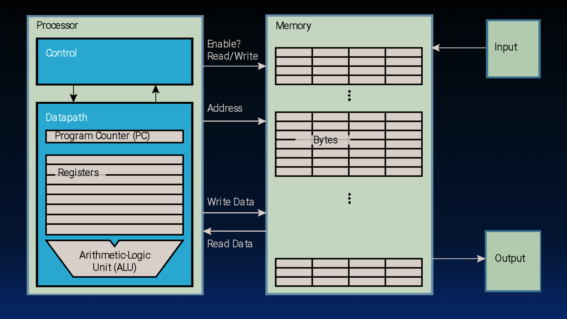
Basic computer layout (See: von Neumann architecture).
Inside the processor, there are two main components:
- Datapath (“the brawn”): The portion of the processor that contains the hardware necessary to perform operations required by the processor. The RISC-V datapath describes the flow of data between core elements of the RISC-V processor.
- Control (“the brain”): The portion of the processor (also in hardware) that tells the datapath what needs to be done. The control describes the signals needed to ensure the elements of the datapath correctly execute a RISC-V instruction.
One analogy comes from the operation of the International Space Station (ISS). The space station is like the datapath that has all the hardware needed to perform operations in space. Mission control is on the Earth and, given some data from the space station, sends directions back to the ISS. Both the space station and mission control have computers (e.g., combinational logic) and state, and both are needed to ensure correct operation of the International Space Station as a system.

The RISC-V datapath is like a space station.

The RISC-V control logic is like mission control.
Single-Cycle Processor
A CPU is a complex digital logic system that updates state using combinational logic. It has two types of elements (discussed in the next section):
- State elements that contain state, e.g., registers, memory, etc.
- Combinational Logic Blocks that operate on data values, e.g., ALU, muxes, combinational logic, etc.
Our goal for this chapter is to design a single-cycle processor that executes one instruction each cycle, starting from fetching the instruction all the way to updating the PC for the next instruction.
- During each clock cycle, the current outputs of the state elements drive the inputs to combinational logic, whose outputs settle at the inputs to the state elements before the next rising clock edge.
- Then, at the rising clock edge, all the state elements are updated with the combinational logic outputs, and execution moves to the next clock cycle.
The Processor as a State Machine?
Theoretically, to design our CPU we could implement something like #fig-monolithic-datapath. We could make a “finite” state machine that considers every instruction as a separate state, then specifies combinational logic for transitioning to every other possible instruction.
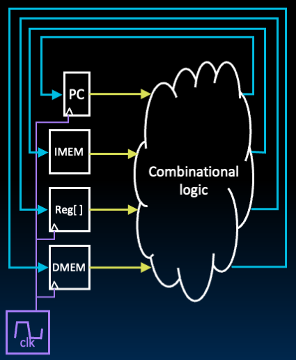
A strawman, bulky approach to implementing our datapath. We discuss the state elements listed in the figure in the next section.
5 Steps to a RISC-V Instruction
Instead of the complicated FSM approach above, we will break up the process into five steps, then connect the steps to create the whole processor circuit. For each instruction, we will determine whether additional logic needs to be incorporated into each phase.
The benefit of this approach is two-fold:
- Smaller steps are easier to design
- Modularity means that we can optimize one step without touching the others.
In the single-cycle datapath, all phases of one RV32I instruction will execute within the same cycle23: Instruction Fetch (IF) starts on the first rising edge of a clock, and Write Back (WB) finishes3 the final result on the next rising edge.
In the next section, we introduce the key elements of a RISC-V datapath. For now, we share #fig-five-step-single-cycle-datapath and let you guess at the meaning of each hardware block.
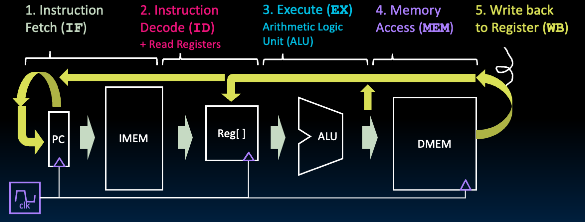
Five steps of a single-cycle datapath. See this section for descriptions of each hardware block.
We emphasize the layer of abstraction between datapath and control with #fig-five-step-single-cycle-control below. The The control logic selects “needed” datapath lines based on the instruction. The control logic specifies if data needs to be written to memory or registers, which arithmetic or logical operation to execute, selectors for MUXes, etc.
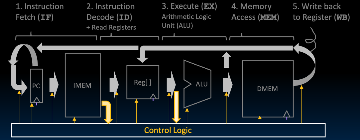
As the datapath computes values, the control logic selects the necessary values needed to execute the instruction.
From P&H Section 4.7:
Finally, we note that this single-cycle approach is not practical, since the clock cycle must stretch to accommodate the slowest instruction that takes all five steps. After designing the single-cycle datapath, we will look at faster implementations that leverage pipelining.
Footnotes
-
It is more accurate to say that during
MEM, we setup the data to store back toDMEMby ensuring that the input toDMEMis stable before the next rising edge of the clock. Then, on the rising edge,MEMstores the correct value to memory. See more: DMEM ↩ ↩2 -
For our single-cycle datapath, it is more accurate to say that during
WB, we set up the value to write back to the Register File by ensuring that the input D of registerrdis stable at setup time, before the next rising edge of the clock. Then, on the rising edge, the registerrdtakes this value, then after a clk-to-q delay, has the correct value on its output Q. See more: RegFile ↩ ↩2 ↩3